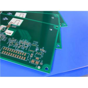
6-Layer PCB with RO4350B and High Tg FR-4 (S1000-2M)
This 6-layer PCB is a robust and versatile solution designed for high-performance RF and microwave applications. Built with a hybrid construction of RO4350B and High Tg FR-4 (S1000-2M) materials, this PCB combines the electrical and thermal advantages of Rogers laminates with the mechanical reliability of FR-4. Below, we analyze the board’s features, advantages, and disadvantages to help you understand its capabilities.

Key Construction Details
| Parameter | Specification |
| Base Material | RO4350B + High Tg FR-4 (S1000-2M) |
| Layer Count | 6 layers |
| Dimensions | 30.55mm x 37.7mm (±0.15mm) |
| Finished Thickness | 1.3mm |
| Copper Weight | 1oz (35μm) for all layers |
| Minimum Trace/Space | 4/4 mils |
| Minimum Hole Size | 0.25mm |
| Blind Vias | L1-L2 |
| Surface Finish | ENEPIG (Electroless Nickel Electroless Palladium Immersion Gold) |
| Solder Masks | Top: None; Bottom: Green |
| Silkscreen | Top and Bottom: White |
| Electrical Testing | 100% tested before shipment |
PCB Stackup
| Layer | Material | Thickness |
| Copper Layer 1 | Copper (1oz) | 35μm |
| Dielectric Layer 1 | RO4350B Core | 0.102mm (4mil) |
| Copper Layer 2 | Copper (1oz) | 35μm |
| Dielectric Layer 2 | Prepreg FR-4 | 0.254mm (10mil) |
| Copper Layer 3 | Copper (1oz) | 35μm |
| Dielectric Layer 3 | FR-4 (S1000-2M) | 0.254mm (10mil) |
| Copper Layer 4 | Copper (1oz) | 35μm |
| Dielectric Layer 4 | Prepreg FR-4 | 0.254mm (10mil) |
| Copper Layer 5 | Copper (1oz) | 35μm |
| Dielectric Layer 5 | FR-4 (S1000-2M) | 0.254mm (10mil) |
| Copper Layer 6 | Copper (1oz) | 35μm |
Advantages
RO4350B Material Properties:
- Provides a low dielectric constant (Dk) of 3.48 ±0.05 and a low dissipation factor (Df) of 0.0037 at 10GHz, ensuring minimal signal loss and excellent RF performance.
- Its high Tg (>280°C) and low Z-axis CTE (32 ppm/°C) improve thermal stability and plated through-hole (PTH) reliability, even under thermal shock conditions.
FR-4 (S1000-2M) Properties:
- Offers excellent mechanical strength, high heat resistance, and anti-CAF performance, which enhances long-term reliability.
- Compatible with lead-free soldering processes and resistant to delamination at high temperatures.
High-Performance ENEPIG Surface Finish:
ENEPIG (Electroless Nickel Electroless Palladium Immersion Gold) is an advanced surface finish that provides:
- Excellent corrosion resistance and long shelf life.
- High solderability for fine-pitch components, making it ideal for RF circuits.
Compact Yet Capable Design:
- With a size of 30.55mm x 37.7mm, the PCB is compact enough for space-constrained applications while supporting complex designs, thanks to its 6-layer construction.
- Blind vias (L1-L2) enable dense circuit integration, reducing board size without sacrificing functionality.
Disadvantages
High Manufacturing Costs:
The hybrid construction with RO4350B and High Tg FR-4, along with the ENEPIG finish, increases production costs compared to standard FR-4 PCBs. This makes it less suitable for cost-sensitive or high-volume applications.
No Top Solder Mask:
The absence of a top solder mask may expose components to environmental factors, requiring extra care during assembly and operation.
Limited Scalability:
With only 8 components, 39 pads, and 23 vias, the design is optimized for specific applications but may lack scalability for more complex circuit designs.
Applications
Commercial Airline Broadband Antennas
Radar and Guidance Systems
Satellite Communications
Phased Array Antennas
Conclusion
This 6-layer PCB is a high-performance, RF-focused solution that combines the benefits of RO4350B’s low-loss dielectric properties with S1000-2M’s mechanical robustness. Its ENEPIG surface finish, compact design, and mixed dielectric stackup make it ideal for aerospace, radar, and satellite communication systems. However, its higher production costs and lack of a top solder mask may restrict its use in more general-purpose or cost-sensitive applications.